𐄀 Focus on providing PCBA separator manufacturing process solution

Quick Answer
Good PCB panelization design should consider the final depaneling process before the panel is released for production. V-score lines, routed channels, breakaway tabs, mouse bites, component keep-out areas, fiducial marks, tooling holes, panel rails, and fixture support can all affect how reliably a PCB panel is processed and separated.
For automated PCB depaneling, the goal is not simply to fit as many boards as possible onto one panel. The panel must remain mechanically stable during SMT and handling while still providing enough access for the router bit, laser path, vision system, fixture, and final separation process.
PCB panelization is the process of arranging multiple individual PCBs into a larger manufacturing panel so they can move through fabrication, solder paste printing, component placement, reflow, inspection, testing, and other production processes more efficiently.
Once assembly is complete, the boards must be separated from the panel. This means panelization and depaneling are not independent processes. Decisions made during panel design can directly influence fixture design, cutting access, mechanical stress, PCB edge quality, cycle time, and automation feasibility.
Eurocircuits' PCB panel guidelines show how panel borders, break routing, V-cutting, fiducials, tooling holes, and board spacing are considered together during panel design. Exact dimensions vary between PCB manufacturers and assembly lines, so the final panel should always be checked against the requirements of the fabricator, assembler, and depaneling process.
One of the most common panelization mistakes is designing the complete panel first and deciding how to separate the boards later. Different depaneling methods require different panel geometry.
| Depaneling Method | Panel Design Requirement | Main DFM Consideration |
|---|---|---|
| Router | Routing channels and tabs between PCB and panel | Tool diameter, router access, tab locations, component clearance and fixture support |
| Laser | Accessible programmed cutting path | Material compatibility, cutting clearance, heat-sensitive areas and fixture strategy |
| V-Score | Continuous straight score lines | Straight board edges and sufficient clearance from components and copper |
| Tab Routing / Mouse Bites | Routed profile with controlled breakaway tabs | Tab quantity, tab position, hole pattern and remaining panel rigidity |
If the separation process has not yet been selected, review our comparison of PCB depaneling methods before finalizing the panel layout.
Panel rails, sometimes called breakaway rails or panel borders, provide additional material around the PCB array. They can help the panel remain rigid during handling, solder paste printing, pick-and-place, reflow, inspection, and depaneling.
Rails also provide space for manufacturing features that may not belong on the finished PCB, including fiducials, tooling holes, barcodes, panel identification, coupons, and fixture reference features.
Important: There is no universal panel-rail width that is correct for every production line. Rail requirements depend on PCB size, panel dimensions, conveyor equipment, assembly machinery, fixture design, component weight, and the PCB manufacturer's process rules.
V-scoring creates grooves on the PCB panel so the individual boards can later be separated along predefined straight lines. It can be highly space-efficient because adjacent PCBs may not require a wide router channel between them.
However, V-score geometry is much less flexible than programmable routing. Score lines generally need to continue along a straight path across the panel, making this approach most suitable for rectangular or straight-edged PCB designs.
Designers should also maintain appropriate clearance between the score region and nearby copper, components, connectors, vias, and other critical features. The exact clearance and remaining material thickness should be defined with the PCB fabricator rather than copied from a generic internet specification.
Altium provides a useful engineering overview of V-score and mouse-bite PCB panel design, including the need to define score locations and maintain clearance around the scoring region.
Tab routing is widely used when the PCB outline cannot be separated using straight V-score lines. Most of the PCB contour is routed during fabrication, while small tabs remain between the individual PCB and the surrounding panel structure.
These tabs keep the PCB mechanically connected to the panel during SMT assembly and handling. During final depaneling, a router machine cuts through the remaining tabs to release the individual board.
When Designing Router Tabs, Consider:
The diameter of the router bit used during final depaneling
Available clearance around the cutting path
The number and position of tabs needed for panel stability
The distance between tabs and sensitive components
The ability of the fixture to support the PCB before the final tab is cut
The cutting sequence and how the PCB will be removed after separation
If the tab width or routing channel has already been defined, router-bit diameter and cutting parameters should be selected accordingly. See our guide to PCB router bits for depaneling for more information.
Mouse bites are rows of small drilled holes placed across or near a breakaway tab. The holes reduce the amount of material that must be fractured when the PCB is manually removed from the panel.
They are especially common in prototype, low-volume, or manually separated panels. However, the hole diameter, spacing, tab width, routing geometry, and hole position should not be selected from a universal template.
Different fabricators use different routing-tool diameters and mouse-bite specifications. The panel drawing should clearly identify the intended routed areas, tab locations, and breakaway-hole pattern so the PCB manufacturer can review the design for manufacturability.
DFM Note: Mouse bites are not automatically required when a panel will be separated with an automated PCB router. For automatic routing, solid tabs that are cut completely by the machine may provide a cleaner and more controlled process. Confirm the intended separation method before adding perforated tabs.
Components placed very close to the board edge can make depaneling more difficult. The cutting tool, fixture, dust-extraction structure, or PCB movement during separation may require more physical space than the board outline alone suggests.
Sensitive components such as ceramic capacitors, BGAs, connectors, sensors, large inductors, shielding structures, and overhanging components should be reviewed carefully when they are located near a router path or V-score line.
The required keep-out distance depends on the PCB structure, depaneling technology, fixture, component height, tool diameter, and mechanical-stress requirement. For this reason, a fixed component-to-edge number should not be applied to every PCB without reviewing the actual manufacturing process.
| Edge Feature | What to Review |
|---|---|
| MLCC / Ceramic Components | Board flex and mechanical stress near the cutting path |
| Connectors | Overhang, fixture interference and cutter access |
| BGA / CSP | Distance from routing tabs and local PCB flex |
| Shielding Covers | Cutter, fixture and dust-collection clearance |
| Heavy Components | Panel sagging, support strategy and tab distribution |
Fiducials are optical reference marks used by automated production equipment to determine panel position, orientation, rotation, and alignment.
They are commonly used during solder paste printing, pick-and-place, AOI, and other vision-guided processes. PCB depaneling equipment with CCD vision can also use reference marks to compare the actual panel position with the programmed cutting coordinates.
Fiducials should be visible to the camera, free from nearby features that interfere with recognition, and located according to the requirements of the assembly and depaneling equipment.
Altium's guide to PCB tooling holes and fiducials discusses how these features are commonly incorporated into panel rails for manufacturing and machine alignment.
For Automated Depaneling: Confirm which fiducials or Mark points the vision system will use before finalizing the panel. A mark that works well for SMT equipment is not automatically the best reference for every depaneling fixture and cutting program.
Tooling holes provide mechanical reference points for manufacturing fixtures and automated equipment. They may be used during PCB fabrication, assembly, inspection, testing, and depaneling.
In panelized production, tooling holes are often positioned in the panel rails so the manufacturing equipment can locate and secure the complete panel without consuming valuable space on the finished PCB.
Hole diameter, tolerance, quantity, and location should be defined according to the actual fixture and assembly-line requirements. Do not confuse manufacturing tooling holes with mounting holes that remain in the finished product.
A panel that contains many routing channels, cutouts, small PCBs, or insufficient tabs can become mechanically weak. It may sag or twist during handling and assembly, creating problems long before the depaneling process begins.
Panel stability becomes especially important when the PCBs contain heavy components or when large areas of material have been removed by routing. Panel rails, tab quantity, board spacing, support points, and overall panel size should therefore be evaluated together.
Eurocircuits also emphasizes mechanical stability when panelizing small PCBs , noting that increasing the amount of routed material can weaken the overall panel.
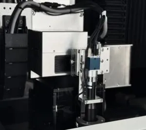
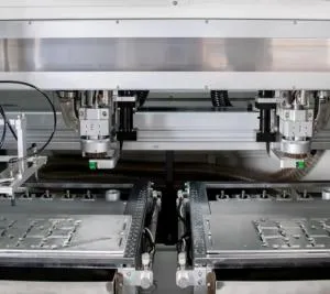
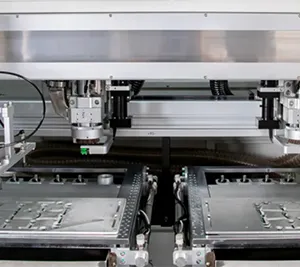
When a panel will be separated with an automated PCB router, the machine must physically access every programmed cutting location. The panel design should therefore account for the router-bit diameter, spindle structure, fixture, dust extraction, and PCB support.
Narrow routing channels or components located very close to the edge can restrict cutter access. At the same time, removing too much material around the PCB can reduce panel stiffness.
An automated router fixture should also support the individual PCB as the final tabs are cut. Without sufficient support, the board can move, drop, rotate, or place unnecessary load on the remaining tabs.
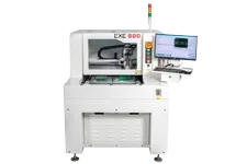
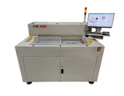
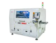
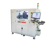
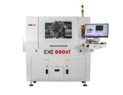
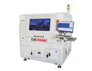
The EXE 880 Offline PCB Depaneling Machine uses programmable router cutting and CCD vision positioning for PCB separation. Panel and fixture design should be reviewed together before production to ensure suitable cutter access and PCB support.
Laser depaneling does not require a mechanical router bit to travel through the panel, but the cutting path still needs to be designed with the actual laser process in mind.
Material type, board thickness, copper near the cut line, component sensitivity, heat-affected characteristics, fixture support, and fume extraction can all influence process design. A panel optimized for mechanical routing should therefore not automatically be assumed to be optimal for laser cutting.
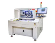
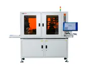
For applications requiring non-contact separation, the EXE 960 Offline Laser Depaneling Machine provides an alternative to mechanical PCB routing.
A clear panel drawing reduces ambiguity between the PCB designer, fabricator, assembler, fixture supplier, and depaneling equipment manufacturer.
Useful Depaneling Data May Include:
PCB and complete panel dimensions
Gerber or ODB++ production data
DXF or mechanical outline files
V-score locations where applicable
Router paths and breakaway-tab locations
Fiducial / Mark-point positions
Tooling-hole locations and dimensions
Component-height and edge-clearance information
PCB material and thickness
Required cutting quality, cycle time, and automation method
| Panelization Mistake | Possible Production Problem |
|---|---|
| Choosing V-score for an irregular board outline | Score lines cannot follow the required contour |
| Components positioned too close to the cutting path | Limited cutter or fixture clearance and increased stress risk |
| Too few breakaway tabs | Panel may become unstable during assembly or handling |
| Too many or oversized tabs | Longer routing cycle and unnecessary material removal |
| Poorly positioned fiducials | Vision recognition and coordinate alignment may become unreliable |
| No clear panel drawing | Fabricator, assembler and depaneling supplier may interpret the design differently |
| Designing the panel without considering the fixture | Insufficient support or interference during automated cutting |
Have you selected the final PCB depaneling method?
Is the panel mechanically stable throughout SMT assembly?
Are panel rails wide enough for the required production equipment?
Are routing channels compatible with the intended router-bit diameter?
Are breakaway tabs positioned where the PCB can be properly supported?
Are sensitive components sufficiently separated from the cutting path?
Are V-score lines compatible with the PCB outline?
Are fiducials visible and compatible with the vision system?
Are tooling holes compatible with the fixture and production line?
Can the cutting tool or laser access every required separation path?
Will each individual PCB remain supported during the final cuts?
Has the complete panel drawing been reviewed by the fabricator, assembler, or depaneling supplier where necessary?
Related Engineering Guide: After the panel design is finalized, cutting quality also depends on machine stability, spindle performance, vision alignment, fixture design and cutting parameters. Learn more in How Does a PCB Depaneling Machine Achieve Clean and Precise Cuts?
PCB panelization is the process of arranging multiple individual PCBs into a larger manufacturing panel so the boards can be fabricated, assembled, inspected, tested, and handled more efficiently before final depaneling.
Tab routing leaves small solid sections of PCB material connecting the board to the panel after most of the outline has been routed. Mouse bites add a row of drilled holes to a breakaway tab so the remaining material can be fractured more easily during manual separation.
There is no universal mouse-bite hole diameter, spacing, or tab width that is correct for every PCB manufacturer. These dimensions depend on the fabricator's routing process, PCB thickness, board size, required panel strength, and final separation method. Use the PCB manufacturer's panelization specification whenever possible.
Generally, V-scoring is best suited to straight PCB edges because the score line normally runs continuously across the panel. Irregular outlines, curved edges, and complex contours are usually better suited to routing or laser depaneling.
The required component-to-edge clearance depends on the component type, depaneling method, PCB material, fixture, router-bit diameter, assembly process, and mechanical-stress limits. Instead of using one universal number, confirm the required keep-out zone with the PCB fabricator, assembler, and depaneling process.
Fiducials provide optical reference points that allow a vision system to determine the actual position and orientation of the PCB panel. The machine can use this information to align or compensate the programmed cutting coordinates before depaneling.
Not necessarily. Automated PCB routers can cut solid breakaway tabs completely, so perforated mouse-bite tabs may not be required. The correct tab design depends on how the panel is assembled, handled, supported, and finally separated.
Useful information includes PCB material, thickness, individual board dimensions, full panel dimensions, panel drawing, Gerber or mechanical files, cutting path, tab positions, component clearance, fiducial locations, expected production volume, and required cycle time.
Good PCB panelization is not simply about maximizing the number of boards per manufacturing panel. The panel must remain stable during assembly while also supporting reliable final separation.
V-score geometry, tab routing, mouse bites, component keep-out areas, fiducials, tooling holes, panel rails, routing channels, fixture support, and cutting access should all be reviewed according to the intended depaneling process.
The most effective approach is to select the depaneling method early and coordinate the PCB designer, fabricator, assembler, fixture supplier, and depaneling equipment provider before the production panel is finalized.
Need Help Evaluating Your PCB Panel Design?
Send EXE your PCB material, thickness, panel drawing, Gerber or DXF files, tab locations, component clearance, production volume, and cycle-time requirement. Our team can help evaluate the panel for router or laser PCB depaneling.
Request a Panel Depaneling Evaluation