𐄀 Focus on providing PCBA separator manufacturing process solution

Quick Answer
PCB depaneling stress describes the mechanical loading and board deformation that can occur while individual PCBs are separated from a panel. One practical way to evaluate this deformation is to attach strain gauges to selected PCB locations and measure strain during the actual depaneling process.
Results are commonly expressed in microstrain (µε). However, there is no single universal µε limit that is correct for every PCB or component. Acceptable limits should be established from customer requirements, component-supplier guidance, applicable test methodology, or validated internal manufacturing criteria.
PCB depaneling is often one of the final mechanical operations performed on an assembled PCB or PCBA. During routing, V-score separation, manual breakaway, punching, or other separation processes, the board can bend, twist, vibrate, or experience localized force.
For many assemblies, the key question is therefore not simply whether the PCB can be separated successfully, but whether the process introduces an acceptable level of strain around critical components and solder joints.
The IPC/JEDEC-9704A Printed Circuit Assembly Strain Gage Test Guideline provides a standardized methodology for measuring printed-circuit-assembly strain and board flexure. It specifically identifies printed board depanelization as one of the manufacturing operations that may be characterized using strain-gauge testing.
The terms stress and strain are often used together, but they describe different physical quantities.
| Term | Meaning | Relevance to PCB Depaneling |
|---|---|---|
| Stress | Internal mechanical force per unit area within a material | May develop as the PCB is loaded, bent, clamped, or separated |
| Strain | Relative deformation or change in dimension of the material | Can be measured directly on the PCB surface using strain gauges |
In manufacturing discussions, people often say “PCB stress measurement,” but the instrumented test commonly measures strain. Those strain results can then be used to assess PCB flexure and the mechanical severity of a production operation.
Strain is the ratio between a change in length and the original length. Because PCB deformation is normally very small, engineers commonly express it in microstrain.
1 µε = 1 × 10⁻⁶ strain
Microstrain provides a convenient way to express very small PCB deformations measured during manufacturing.
Micro-Measurements provides a useful explanation of mechanical strain, microstrain, and strain-gauge measurement, including how small resistance changes in a bonded strain gauge can be used to measure deformation.
A PCB can appear visually normal after depaneling even though the assembly experienced significant flexure during the process. Strain measurement provides quantitative data that can be compared before and after process changes.
Compare different PCB fixtures or support strategies.
Evaluate different breakaway-tab positions or panel designs.
Compare cutting sequences and routing directions.
Evaluate the effect of router-bit condition or cutting parameters.
Compare manual, router, laser, or other separation processes.
Establish a measurable baseline for future process improvement.
Kyowa's PCA strain and stress measurement resources specifically identify PCB depaneling as an application for strain measurement and provide measurement systems designed around IPC/JEDEC-9704A methodology.
Strain gauges should not simply be placed wherever there is free PCB space. Measurement locations should be selected according to the purpose of the test, component layout, expected bending direction, depaneling path, and areas considered mechanically critical.
IPC/JEDEC-9704A discusses strain testing for assemblies containing surface-mount devices such as BGA, CSP, SOP, and area-array connectors or sockets, and notes that the approach may also be applicable to discrete SMT devices such as capacitors and resistors.
| Area to Evaluate | Why It May Matter |
|---|---|
| Near BGA / CSP Packages | Board bending near area-array packages may be important when validating mechanical manufacturing processes. |
| Near Connectors | Connector installation, board-edge location, and fixture interaction can influence local flexure. |
| Near Breakaway Tabs | The final remaining tabs can concentrate load as the board becomes progressively less supported. |
| Large Unsupported Areas | Large spans may bend more easily if fixture support is insufficient. |
| Near the PCB Edge | Routing paths, V-score lines, tabs, and component clearance can create localized process sensitivity. |
A strain-gauge test should reproduce the real manufacturing operation as closely as practical. The objective is to record PCB deformation while the board goes through the actual fixture, loading, cutting, release, and handling sequence.
Step 1 — Define the Test Objective
Determine which production step, component area, fixture design, or depaneling condition needs to be evaluated.
Step 2 — Select Measurement Locations
Choose locations based on critical components, expected flexure, panel geometry, fixture support, and the purpose of the evaluation.
Step 3 — Install the Strain Gauges
Prepare the PCB surface and bond the selected strain gauge according to the measurement procedure and gauge manufacturer's instructions.
Step 4 — Record the Actual Depaneling Cycle
Run the instrumented PCB through the same loading, positioning, cutting, release, and unloading process used in production.
Step 5 — Analyze Strain and Strain Rate
Review maximum strain, principal strain where applicable, strain direction, strain rate, and the point in the manufacturing sequence where the largest event occurs.
Step 6 — Compare Against the Approved Criteria
Compare results with limits established by the customer, component supplier, applicable engineering guideline, or internally validated process criteria.
Maximum strain is not always the only useful result. Strain rate describes how quickly strain changes over time. A rapid mechanical event and a slow board deflection can therefore produce different test signatures even if their peak strain values appear similar.
This is why a useful depaneling evaluation records the complete time history rather than only one maximum µε number. The time-series data can help identify whether a peak occurs during clamping, router entry, tab cutting, final board release, pickup, or another handling step.
| Factor | Potential Effect |
|---|---|
| Fixture Support | Insufficient or poorly distributed support can allow the PCB to move, bend, or vibrate during cutting. |
| Tab Position | Tab location affects how load is distributed as the PCB becomes progressively separated from the panel. |
| Cutting Sequence | Cutting tabs in a different order can change the amount and location of remaining PCB support. |
| Router Bit Condition | Tool wear can change cutting force, vibration, and edge quality. |
| Feed Rate & Routing Parameters | An unsuitable process recipe can increase cutting load or vibration. |
| PCB Thickness & Geometry | Board stiffness and response to mechanical loading vary with panel and PCB construction. |
| Component Location | Components close to tabs, score lines, or unsupported edges may require additional process evaluation. |
| Final Board Handling | Strain can occur not only during cutting but also when the separated PCB is lifted, removed, or transferred. |
Panel Design Matters: Tab positions, router channels, component clearance, fiducials, tooling holes, and panel rigidity can influence the depaneling process. Review our PCB Panelization Design for Automated Depaneling .
If strain testing identifies an undesirable mechanical event, the best corrective action depends on where and when the peak occurs. The following process variables are common areas to investigate.
Improve PCB Support: Adjust fixture contact areas so the PCB remains supported near the active cutting region and during the final separation steps.
Optimize the Cutting Sequence: Review which tabs are cut first and which remain until the end so the board does not lose critical support too early.
Monitor Router Bit Condition: Worn or damaged cutters can increase cutting force and vibration. Tool-life management should therefore be included in process control.
Validate Feed Rate and Spindle Parameters: Cutting parameters should be qualified on the actual PCB rather than optimized only for maximum machine speed.
Review the Panel Design: Tab location, panel rigidity, routing-channel design, and component clearance should support the intended automated depaneling process.
Retest After Process Changes: Repeating the strain measurement after modifying the fixture, cutting path, tool, or process recipe provides objective evidence of whether the change improved the result.
Related Router Guide: Learn how cutter diameter, spindle speed, feed rate, and tool wear affect the PCB routing process in our PCB Router Bits for Depaneling Guide.
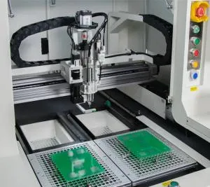
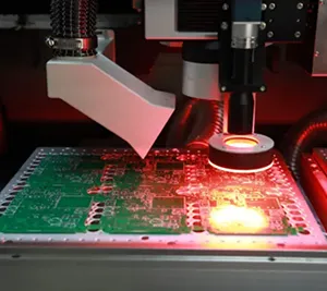
Router depaneling uses a mechanical milling cutter, so PCB support, tool condition, cutting parameters, and routing sequence can influence the mechanical load applied during separation. With an optimized process, router systems can achieve controlled low-stress separation across many rigid-PCB applications.
Laser depaneling uses non-contact material removal and therefore does not apply router-bit cutting force to the PCB. However, laser processing introduces a different set of considerations, including material compatibility, thermal effects, cutting speed, fumes, and process cost.
For a broader comparison of router, laser, V-cut, punching, and other processes, see our PCB Depaneling Methods Comparison.
Equipment specifications can provide useful process information, but a machine-level stress value should not automatically be treated as the universal acceptance limit for every PCB assembly.
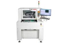
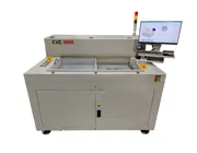
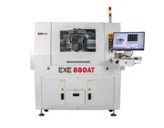
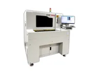
For example, the EXE 880 Offline PCB Depaneling Machine publishes a board-separation stress specification of below 300 µε. This is a specification associated with that machine and its defined test conditions; it should not be interpreted as a universal allowable strain limit for every PCB, BGA, capacitor, solder joint, or automotive or medical electronic assembly.
Important: IPC/JEDEC-9704A describes a methodology for strain-gauge testing; it does not provide one universal pass/fail strain number for every assembly. Acceptance criteria may come from customers, component suppliers, or validated internal engineering practices.
Automotive Electronics
ECU, ADAS, BMS, EV power-control, and other automotive PCBs can contain dense layouts and mechanically sensitive areas. Strain measurement can help manufacturers compare fixtures, cutting sequences, and separation processes during process validation. Explore PCB depaneling solutions for automotive electronics.
Medical Electronics
Medical PCB assemblies may also require controlled manufacturing processes and repeatable PCB separation. Actual strain limits and validation criteria should be established according to the specific product and quality requirements. Learn more about PCB depaneling for medical electronics.
Define which component areas or PCB locations are mechanically critical.
Confirm the approved strain and strain-rate acceptance criteria.
Select strain-gauge locations according to the test objective.
Reproduce the real production fixture and depaneling sequence.
Record the complete loading, cutting, release, and unloading process.
Identify exactly when the maximum strain event occurs.
Evaluate fixture support and final-tab cutting sequence.
Check router-bit condition and validated cutting parameters.
Repeat the measurement after process changes.
Keep test conditions and results documented so future production changes can be compared against the same baseline.
PCB depaneling stress refers to mechanical loading that occurs while a PCB is separated from a production panel. Engineers often evaluate the resulting board deformation by measuring PCB strain with bonded strain gauges.
µε means microstrain. One microstrain represents one millionth of strain, or 1 × 10⁻⁶. It is commonly used because the dimensional changes measured on PCBs are very small.
There is no single universal PCB strain limit suitable for every assembly. Acceptance criteria should be based on customer requirements, component-supplier guidance, applicable engineering standards, or a validated internal manufacturing specification.
Yes. Strain gauges can be attached to selected PCB locations and connected to suitable data-acquisition equipment while the instrumented assembly goes through the real depaneling operation.
A worn cutter can change cutting force, vibration, and routing behavior, so tool condition is one variable worth evaluating when strain or edge quality changes. The effect should be confirmed through actual process measurement rather than assumed from tool age alone.
Laser cutting is non-contact and does not apply router-bit cutting force to the PCB. However, the complete production process still includes fixturing, handling, loading, unloading, and material-specific laser effects, so the overall application should still be validated.
No. Below 300 µε is a published board-separation stress specification for the EXE 880 under its defined equipment conditions. It should not be treated as a universal acceptance criterion for every PCB assembly or component.
PCB depaneling strain measurement converts a subjective concern about board flex into measurable process data. By recording strain during the real manufacturing cycle, engineers can identify when PCB deformation occurs and compare the effect of fixtures, tab positions, cutting sequences, router-bit condition, process parameters, and alternative depaneling technologies.
The objective should not be to chase one universal microstrain number. A stronger approach is to define appropriate acceptance criteria for the actual product, establish a repeatable measurement method, and use the results to validate process improvements.
Need to Evaluate PCB Depaneling Stress?
Send EXE your PCB material, thickness, panel drawing, tab locations, component-clearance information, production volume, and depaneling requirements. Our team can help evaluate a router or laser PCB depaneling process for your application.
Request a PCB Depaneling Evaluation