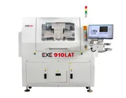
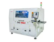
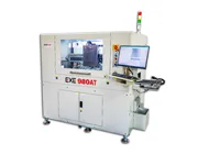
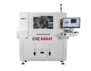
𐄀 Focus on providing PCBA separator manufacturing process solution

LASER DEPANELING MATERIAL SELECTION
A PCB Is Not Just “One Material”
Asking whether a PCB can be laser depaneled sounds like a simple question. In practice, the answer depends on much more than whether the board is labeled FR4, FPC or rigid-flex.
A PCB cutting path may pass through resin, glass reinforcement, polyimide, copper, coverlay, adhesive, solder mask or other layers. Each material interacts with laser energy differently. For this reason, laser depaneling should be qualified from the actual PCB stack-up and cut location rather than from the board category alone.
Two PCBs described as “FR4” can have different resin systems, glass styles, copper distributions, solder-mask systems and total thicknesses. Two flexible circuits can use different polyimide films, adhesive systems and copper thicknesses. A rigid-flex PCB can contain several material interfaces within a very small cutting area.
For example, Isola's FR408HR material information describes an FR-4 resin system reinforced with electrical-grade glass fabric. This illustrates why “FR4” describes a material family rather than one universal laser-processing recipe.
Material compatibility is really a process-window question
The useful question is not only “Can a laser cut this material?” It is whether the selected laser configuration and process parameters can produce the required edge quality, dimensional accuracy, thermal condition and production speed on the actual PCB.
| PCB Type | Typical Material Structure | Why Laser May Be Considered | What Must Be Qualified |
|---|---|---|---|
| FR4 PCB | Glass-reinforced resin laminate, often combined with copper and solder mask | Non-contact processing, narrow or complex cutting geometry and reduced mechanical cutting force | Resin/glass composition, thickness, copper near the cut, thermal effects, edge condition and processing speed |
| FPC / Flex PCB | Commonly polyimide-based flexible substrate with copper and coverlay / adhesive layers | Fine contours, flexible material handling and no mechanical router-bit force at the cutting point | Polyimide grade, copper, adhesive, coverlay, flex thickness, edge discoloration and fixture/support method |
| Rigid-Flex PCB | Combination of rigid and flexible materials with transition and bonding interfaces | Useful to evaluate where mechanical force, tight geometry or sensitive rigid-to-flex transitions are concerns | Exact stack-up, location of the transition, adhesives, copper, flex layers, cut path and thermal response |
FR4 is widely used for rigid PCBs, but laser processing has to deal with a composite rather than a single homogeneous material. The resin and glass reinforcement do not necessarily respond identically to the same laser energy.
That means a process developed for one FR4 construction should not automatically be copied to another board without validation. Resin formulation, glass content, laminate thickness and additional materials close to the cutting path can all change the useful process window.
Glass Reinforcement
FR4 contains glass reinforcement within a resin system, so the cut path passes through materials with different optical and thermal behavior.
Resin System
Different laminate products use different resin formulations. Edge color, ablation behavior and the appropriate energy input should therefore be confirmed on the actual material.
Copper Near the Separation Path
Copper location and thickness may change how energy is absorbed and conducted around the cut. A bare laminate trial is not necessarily representative of a finished PCB.
Board Thickness
Increasing thickness generally increases the amount of material that must be removed. It can affect the required number of passes, cycle time and resulting cut-wall condition.
Flexible printed circuits are commonly built around polyimide films, often combined with copper, adhesive and coverlay layers. One reason laser cutting is frequently considered for flex circuits is that there is no rotating router bit physically pushing against the flexible substrate during separation.
Polyimide itself can be compatible with laser ablation. For example, DuPont's Kapton EN technical data specifically identifies the film as laser ablatable. However, a finished FPC contains more than the base film, so this does not establish one universal setting for every flexible PCB.
For a finished FPC, qualify the complete cut stack
The fixture and support strategy also matter. A thin flexible circuit can move, curl or deform during handling, so cutting performance cannot be separated completely from positioning and material support.
Rigid-flex boards require more careful qualification because the PCB may combine rigid laminate, flexible polyimide, copper and bonding materials within one structure.
The All Flex rigid-flex design reference notes that flex layers typically use polyimide while the rigid sections can use FR4 or polyimide constructions. Consequently, “rigid-flex” is not one homogeneous cutting material.
The rigid-to-flex transition deserves special attention
A trial cut should identify whether the programmed separation path passes through:
• only rigid laminate,
• only the flexible section,
• adhesive or coverlay layers, or
• a transition containing multiple materials.
This is why a process that produces an acceptable edge on the rigid region should not automatically be assumed to produce the same result at a rigid-flex transition.
Special PCB substrates should be treated as separate applications rather than grouped automatically with standard FR4. Ceramic substrates, insulated metal substrates, CEM materials and RF/high-frequency laminates can differ substantially in thermal conductivity, optical absorption, filler content and layer construction.
Do not assume machine compatibility from a generic material name. If a machine supplier has not validated your specific ceramic, metal-core or high-frequency laminate, the correct approach is sample testing rather than copying parameters from FR4 or polyimide processing.
Laser Wavelength and Source
Different materials absorb laser energy differently. A process developed on one laser source should not automatically be transferred to another wavelength or pulse regime.
Total Material Thickness
Thicker stacks generally require more material removal and can alter pass count, processing time and thermal accumulation.
Layer Stack-Up
Copper, glass reinforcement, adhesives, coverlays and resin systems can create different responses along one cutting path.
Cutting Speed and Pass Strategy
Process speed cannot be evaluated independently from energy input and pass count. Faster is not automatically cleaner or more economical.
Required Edge Quality
Acceptable discoloration, heat-affected condition, dimensional tolerance and surface cleanliness depend on the application and should be defined before optimization.
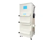
Fume and Particle Extraction
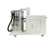
Laser ablation generates process by-products that must be removed from the cutting area. Extraction performance is part of process qualification, not an optional afterthought.
“≤2 mm” Does Not Mean “Every PCB Below 2 mm”
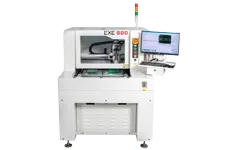
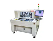
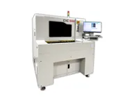
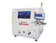
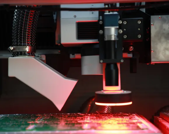
The published specification for the EXE 960 Offline Laser PCB Depaneling Machine lists a machinable material thickness of ≤2 mm.
This should be treated as a machine specification, not as blanket approval for every FR4, FPC, rigid-flex or specialty PCB below that thickness. Material construction, cutting geometry, laser configuration and required output quality must still be validated.
Successful separation is only the first test. A useful material-compatibility trial should evaluate the condition of the finished PCB and whether that result remains stable over repeated cuts.
| Check | What to Inspect | Why It Matters |
|---|---|---|
| Cut Edge | Roughness, discoloration, residue and local damage | Indicates whether the process window meets the required finished-edge condition |
| Dimensions | Final outline and critical dimensional features | Confirms whether the cut follows the required geometry consistently |
| Thermal Condition | Heat-affected appearance close to the cutting path | Helps determine whether energy input and pass strategy require further optimization |
| Adjacent Copper / Features | Copper, pads, traces and components near the cut | Confirms adequate process clearance around functional features |
| Repeatability | Results across multiple panels rather than one sample | One acceptable cut does not establish a stable production process |
| Cycle Time | Validated processing time per panel | A technically acceptable cut must also fit the required production capacity |
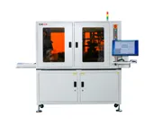
Whether the final equipment is offline or inline does not change the need to qualify the laser-material interaction. First confirm that the required PCB can be processed at acceptable quality and speed; then determine how that cutting process should fit into production.
Offline Laser Depaneling
Useful to evaluate where standalone operation, flexible loading and product changeovers are important.
Inline Laser Depaneling
Useful to evaluate after the laser process has been validated and automated feeding, cutting and output are required.
Instead of choosing a laser machine from a material name, use the actual production board to develop and validate the process.
Identify the Exact Material Stack
Record substrate type, total thickness, copper construction, coverlay, adhesive, solder mask and any special layers within the intended cutting path.
Review the Cutting Drawing
Check contour geometry, cutting length, copper clearance, rigid-flex transitions and the location of nearby components.
Establish an Initial Laser Process Window
Laser configuration, focus, motion strategy, energy input and pass strategy should be developed for the real PCB rather than copied from another material.
Inspect the Cut, Not Just the Separation
Evaluate edge quality, dimensional accuracy, discoloration, residue, nearby functional features and any application-specific acceptance requirements.
Repeat the Trial
Process several representative panels so repeatability can be evaluated instead of approving the process from one successful cut.
Measure Production Cycle Time
Confirm whether the validated process also meets required takt time and production capacity before final machine configuration.
Laser is only one PCB separation method. If the board is technically suitable for laser processing but production cost, thickness or cycle time makes another process attractive, compare router, laser, V-cut, punching and sawing PCB depaneling methods before final equipment selection.
FR4 can be evaluated for laser depaneling, but the correct process depends on the specific laminate construction, thickness, copper near the cutting path, laser configuration and required edge quality. “FR4” alone is not enough information to define the process.
Laser processing is commonly evaluated for flexible circuits because it is non-contact and can follow fine programmed contours. However, the complete FPC stack — including polyimide, copper, adhesive and coverlay — must be qualified rather than evaluating only the base film.
Rigid-flex boards can be candidates for laser depaneling, especially where non-contact processing and complex geometry are important. The actual cutting path and rigid-to-flex material transitions should be tested because several materials may be present within one stack.
No. Thickness affects processing difficulty and cycle time, but material composition, copper distribution, adhesives, cutting geometry, laser configuration and edge-quality requirements also need to be considered.
The best laser parameter begins with the actual PCB
FR4, FPC and rigid-flex are useful starting classifications, but they are not complete laser-processing specifications. The same board category can contain different materials, thicknesses and layer interfaces.
A reliable selection process therefore starts with the PCB stack-up and cutting drawing, develops a material-specific laser process window, inspects repeated trial cuts and finally checks whether the qualified process can meet production cycle-time requirements.
Want to Know Whether Your PCB Is Suitable for Laser Depaneling?
Send EXE your PCB material or laminate designation, total thickness, stack-up information, panel drawing, cutting path, copper clearance, component locations, required edge quality and production-volume target. A sample-cut evaluation can help determine whether laser depaneling should be considered before the machine configuration is finalized.
Request a Laser Cutting Evaluation